
Designing a Nixie HV supply part 1
Backstory
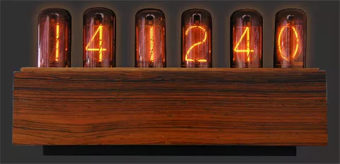
Well basically the backstory is the introduction but shht :). Recently I designed a small PCB with an analog switch for my internship project. This made me remember, I still have to finish my PCB I was doing for my nixie tube clock. Don’t know what those are? Well, here is an example:
I noticed that a huge area was taken by the high-voltage (HV) supply. It is a NCH6100HV, which I bought a couple years ago… The voltage is changeable by a potentiometer, great to experiment with. I was motivated to make it smaller but not only that. During the previous design process, I noticed creating your supplies is something any electronics project is needed. In my case I couldn’t use the very efficient switch-mode power supplies (SMPS) on my small analog switch PCB, as these typically have a lot of switching noise. They would be ideal as you can easily go up in voltage (boost) or down (buck). This made me intrigued but I couldn’t spend time to explore this. Well, during my New years break however, that means project time!
Interwebs, a gold mine
I remember few years ago reading about these supplies being made by hobbyist. So I re-googled these projects and they became a great resource for my nixie tube HV supply. I mainly used these resources:
- de Smith focusses mainly on layout
- Jan Rychter focusses on general design specifications
- 0x7d includes some general information about a few working principles of SMPS
Having scanned over these great projects it was time to dive into the theory.
Working principle of SMPS
The goal is to create a DC high-voltage supply from a lower voltage supply. Just like climbing a mountain going up is a bit more difficult than going down. An example, a bad one however, is to create a lower voltage is using a so called voltage divider. If the load isn’t too heavy its fine but due to the fixed output impedance of the resistive ladder it will be easily disturbed by its load.
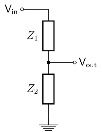 From wikipedia, here \(V_{out}=\frac{Z_2}{Z_1}V_{in}.\)
But the question was how to go up. Well the most common way to step up a DC voltage is to use a boost configuration and is in its simplest sense the following circuit.
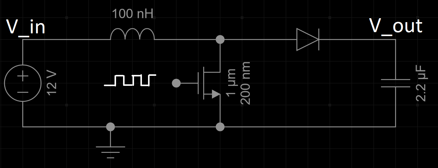
The MOSFET acts as an on/off switch. Initially it is switched on, a certain current will set. When it is switched off, the current has less “way” to flow. The only path is to go through the diode and capacitor. Basically the impedance to the right of the inductor has increased, the current want to decrease. However the inductor tries to counter this, the magnetic field it built up doesn’t want to change. It will increase the voltage to keep the current the same. Ohm’s law with impedance (\(I = V/Z\)) tells, to keep I the same for larger Z we need to increase V. Indeed the constitutive relation of an inductor, \(V=-L\frac{\mathrm{d}I}{\mathrm{d}t}\), tells for decreasing current \(\frac{\mathrm{d}I}{\mathrm{d}t}<0\) , there is a positive voltage, two voltage sources in series add up. This charges the capacitor to higher voltages than the input. In order to prevent the charge from flowing back -which is required to build a higher output voltage- a diode is required.
How do we determine the output voltage?
The output voltage is simple for continuous mode (CCM) and more complex when the converter is in discontinuous mode. Discontinuous mode (DCM) commonly occurs under light loads, as the current is low and quickly falls off to zero. In CCM it is determined solely by the duty cycle (D<1), \(V_{out}=\frac{V_{in}}{1-D}\). As said before in DCM, it is more complex and determined as well by the inductance, the load and switching frequency\(\left(V_{out}=\frac{1+\sqrt{1+\frac{4DR_{load}}{2Lf}}}{2}\right)\).
CCM VS DCM
Although DCM seems more complex, due to the feedback of DC-DC boost controllers, the design is actually easier. All you need to set the output, is to sense the output. For CCM you need to ensure the current through the inductor doesn’t fall to zero. However in DCM the inductor fully cycles in current levels and therefore leads to higher peak currents. These higher peak currents require higher component ratings, lead to decreased lifetime and power efficiency.
But first…
I didn’t want to repeat existing designs, that I could just copy from the internet or datasheets. I went out to research different topologies. You will find typically find the following DC-DC converter topologies.
| Topology | Characteristics | Advantage | Disadvantage |
|---|---|---|---|
| Boost | Go up in voltage | most simple | efficiency by simplicity |
| SEPIC | Go up and down in voltage | non-inverting | complexity |
| Buck-boost | Go up and down in voltage | can go down in voltage | inverting |
| Ćuk | Go up and down in voltage | continuous current | inverting |
The Ćuk topology was intriguing as it could nicely operate in CCM mode, however it was inverting requiring even more components than boosts. The others only added going down in voltage which would be handy in applications which are for example battery powered. Here you start with larger voltage, this decreases over time and you need to switch from going down in voltage to going up. This then requires your topology to support both conversions. But in my case this is unnecessary as it will be powered from a wall adapter and step up to very high voltages.
What then?
Well I don’t dislike reading papers so I just googled and came across so called charge pumps the research community really like these as these can have very high efficiencies and don’t require inductors such as in the boost topology. For more info on these click here. Sadly, this topology would require a lot of stages in order to boost 12 V to 180 V, although not a problem when doing an integrated design. I am building a PCB with discrete components and needing tens of capacitors is non-ideal.
Is all hope lost?
Do I have to settle with the regular boost topology? I guess. It is very simple and I like simple things, as even the simple things can turn out to be difficult. So Keep It Simple Stupid (KISS). The main element in boost converters is the inductor, there are typically 2 versions. The non-isolated (see Jan Rychter) and isolated version (0x7d). The isolated version uses an transformer and doing this has many advantages. It separates the input circuit and output circuit, however note that the ground is still common. But the intrinsic gain transformers can have is much more interesting for me. Since the power in these converter is going to be below 20 W. Those don’t really require galvanic isolation. The intrinsic gain relaxes various design parameters. The gain of the DC-DC converter is relaxed. Stepping up 12 V to 180 V requires a gain of 15 and this means in CCM mode requires a duty cycle of ~93%. This raises a few issues, boost controllers have a minimum on/off time, a minimum frequency and a maximum duty cycle. Lets have a look into this.
Math?!
Well yeah to do some good engineering, math always plays game. But that will be for part 2.
Comments