
Designing a Nixie HV supply part 2
The 160 V Nixie power supply design WORKS
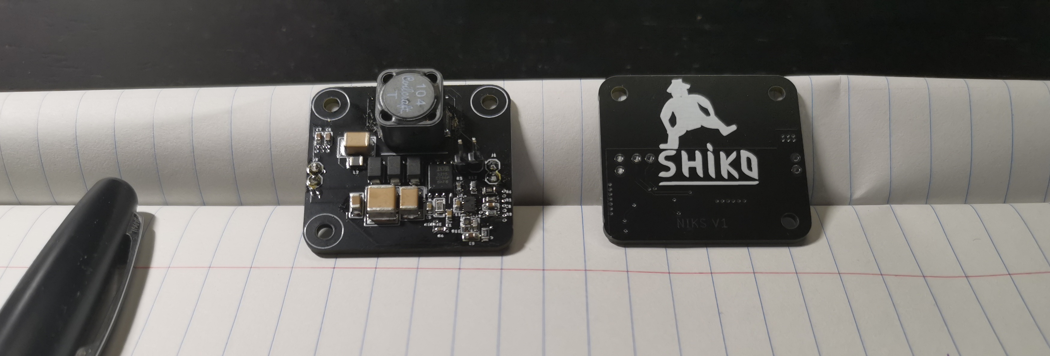
Let’s firstly state the design you will read works without issue. The high voltage nixie power supply has been working in my nixie tube clock (this will be a post later) for about half a year. No issues, as expected from the efficiency and the negligible heating of the components. I have to admit, it rarely happens that a design works on the first try without some modifications…
The Nixie tube power supply has an energy efficiency of 87%
High efficiency is important because a low efficiency implies that the circuit will become hot. Luckily this is not the case due to the good efficiency of 87% at 12 V input. And only ~13% of the energy put into the circuit is turned into heat. I loaded the circuit with various resistors at a 12 V input, the results are summarized in the table below. With V for voltage, I for current, P for Power, and Eff for efficiency.
| V_in | I_in | P_in | V_out | I_out | P_out | \(\eta\) |
|---|---|---|---|---|---|---|
| 11.94 | 0.09 | 1.05 | 158.917 | 0.005 | 0.87 | 83.4% |
| 11.89 | 0.17 | 1.98 | 158.817 | 0.011 | 1.69 | 84.9% |
| 11.83 | 0.25 | 2.96 | 158.917 | 0.016 | 2.56 | 86.5% |
| 11.77 | 0.33 | 3.91 | 158.917 | 0.021 | 3.37 | 86.1% |
| 11.70 | 0.44 | 5.10 | 147.17 | 0.030 | 4.38 | 85.8% |
The wires used to power the circuit had a non-negligible resistance, therefore Kelvin probes were used to determine the potential at the input of the circuit. The maximum output power is around 4 W, which should be able to power 10 bulbs of IN-14. In the last row, at 4.4 W output power, the voltage is lower than the nominal value of 158.9 V.
The output power is limited by the inductor
As mentioned in part 1, the voltage over the inductor is proportional to the inductance and change in current. For higher output power the change in current is larger and this has to be countered with a larger inductance. Unfortunately, by increasing the current through an inductor the inductance actually decreases! This is because the magnetic domains inside the magnetic core of an inductor align with the magnetic field. This was not unexpected as the main two parameters of an inductor, are the inductance and the saturation current. The saturation current was 2 A and is the value where the inductance is greatly reduced from its nominal value.
What do I want?
I need a high voltage supply for my nixie tubes.
- Output voltage of 160 V
- Output current of at least 12 mA (6x IN-14)
- Not noisy
- Does not blow itself up
- Efficiency > 80%
- Voltage ripple <1%
As shown in the basic schematic in part 1, the core components are the inductor, switch (MOSFET), diode and capacitor.
Inductor choice
So how did I choose my inductor, well I looked at which kind of inductors were typically available and this results in an inductor of 100 \muH with a saturation current of 2 A. Trying to buy ones with a larger inductance is either very expensive, physically large, or has a low supply. Now we have to make sure the peak current is below that of the saturation current. The peak current is mainly decided by 2 terms, one which is the output current and the other term is due to the inductor.
\(I_{peak} = I_{in} +\frac{V_{in}D}{2Lf}= 0.25 + \frac{12\cdot0.85}{2\cdot100\cdot10^{-3}} \approx 0.5\) A
The input current (\(I_{in} = \frac{P_{out}}{\eta V_{in}}\)) can be a rough estimate with your target efficiency. Furthermore, choosing an oversized inductor also prevents going into CCM mode. The design of a CCM mode boost converter is difficult here. Because it requires you to have a minimum load, which is not always the case. The bulbs could be turned off or have PWM dimming, which in CCM is hard to achieve due to the low (temporary) load.
Inductor power loss
An inductor is just a long strand of wire, hence it has a resistance \(R_L\) and thus DC power losses. Also changing the magnetic field in the core material can lead to AC losses. These are, \(P_{L,DC} = I_{in}^2 R_L,\)
\[P_{L,AC} = I_{ripple}^2k_1\sqrt{f},\]with \(k_1\) a coupling coefficient from the datasheet:
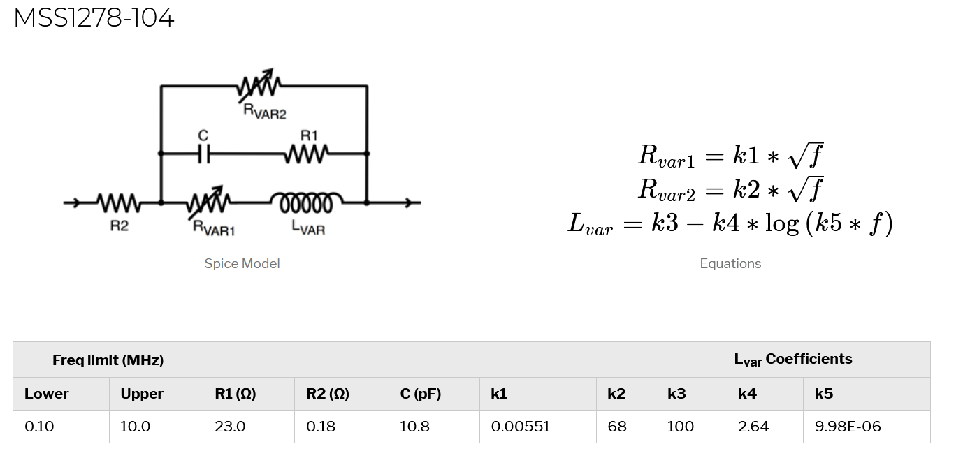
I ignore R1 because the switching happens at 220 kHz and due to the series capacitance in the branch of R1 very little current flows. The impedance of the capacitor is ~\(67\:k\Omega $, while the inductor is ~\)138:\Omega$.
MOSFET switch choice
In order for a boost converter to work, the circuit needs to be in two states. One which easily conducts current and one which hardly conducts any current, this behavior can be achieved using a switch. The choice of MOSFET is important as an ill choice would lead to large energy losses and this leads to low efficiency. The 3 main loss mechanisms are conduction, switching, and gate charging.
Conduction losses
The beauty of semiconductors is that these materials can change from very resistive to almost no resistance -metal-like material- (this is why they can act as switches). Since the resistance is not zero, there are resistive losses which go as, \(P_c=R_{DS,on}I_{peak}^2D,\) with \(R_{DS,on}\) the resistance when the switch is “on” and \(D\) the duty cycle.
Switching losses
During the switching, the current needs to fall or rise. Effectively this means the energy required for changing the current is lost. \(P_{switch}=\frac{1}{2}(V_{out}+V_f)I_{peak}(t_{rise}+t_{fall})f,\) with \(V_f\) the diode forward voltage.
Gate charge losses
In order for a MOSFET to conduct, charges are collected on the gate (\(Q_{gate}\)) to create an electric field. The charges on the gate can be assumed to be lost after discharging it to close the gate again. The power lost through the gate (\(P_{gate}\)) is, \(P_{gate}=Q_{gate}V_{in}f.\) All these losses, typically scale with the size of the MOSFET, so we would like to use a very small MOSFET. Unfortunately, this is not possible because we would like the MOSFET to be resistant to a large difference between the source and drain. Because of the large output voltage, we would need a large MOSFET. It is worth noting that bigger MOSFETs are more expensive. This led me to use a voltage multiplier cell which would let me use the smaller brother of the Infineon IRFH5025, the Infineon IRFH5215.
| Model | \(V_{DS,max}\) (V) | \(Q_{gate}\) (nC) | \(R_{DS,on}\) (m\(\Omega\)) | \(t_{rise}\) (ns) | \(t_{fall}\) (ns) | \(t_{total}\) (ns) |
|---|---|---|---|---|---|---|
| AP15T15GH-HF | 150 | 24 | 150 | 12 | 4 | 16 |
| IRF7853 | 100 | 28 | 15 | 6.6 | 6 | 12.6 |
| IRFH5025 | 250 | 37 | 84 | 6.3 | 6.1 | 12.4 |
| IRFH5215 | 150 | 21 | 58 | 6.3 | 2.9 | 9.2 |
Which in all the listed specs is superior except the maximum voltage between source and drain. The IRFH5215 -is also half the price of IRFH5025- priced at €0.96 (MQTY. 4000). It should be noted the maximum drain current can be a limiting factor, however for power MOSFETs as these, this is generally not a problem and is much higher than the inductor saturation current.
Diode
The diode is there to prevent the capacitor from discharging. However, each time current passes the diode there are two losses: forward voltage drop power loss and switching losses again.
“Diode resistance”
Because the voltage is decreased after a diode, there is a power loss (\(P_{f}\)) attributed to this as current is passing. This current is roughly, on average \(I_{avg} = P_{out}/V_{in}\). \(P_f = (1-D)V_fI_{avg},\) with \(V_f\) the forward voltage drop of the diode. In order to improve the efficiency of my design, I could change the design to a synchronous boost controller, which means replacing the diodes with a MOSFET as the voltage drop along the channel is much smaller than a diode. However, this adds a lot of complexity and cost, as a MOSFET is more expensive and needs to be driven. Also, the impact of this voltage drop is low because of the large boost ratio (\(V_{out}/V_{in}\)) and large output voltage.
Switching losses in diodes
The switching loss in diodes is due to the reverse recovery current. My simulation shows that this only contributes very little to the overall power loss. Please read the link for a full discussion.
Discussion on voltage ripple
In some applications, such as in ADC and DAC the voltage reference should be as noise free as possible. It is then important to have a low voltage ripple as you try to keep your error as small as possible. However, in nixie tubes this is not really an issue as they can be (in principle) driven by your AC wall output. Nevertheless, you would like the apparent brightness not to change too much so I arbitrarily chose the ripple to be within 1%. An easy fix would be to oversize de the inductor which I did, or to increase the output capacitor. In the latter case, it acts as a battery and since it will be able to store more energy the drop in voltage would be less if more energy is stored and the same amount is taken out every time.
Total power loss
The efficiency (\(\eta\)) is just \(P_{out}/P_{in}\). In other words, \(\eta = \frac{P_{in} - P_{loss}}{P_{in}},\) with, \(P_{loss}=P_{L,DC}+P_{L,AC}+P_c+P_{switch}+P_{gate}+P_f.\) The expected efficiency of my design was 89%, which is a bit higher than the measured one. The 2% difference can already be explained if I have ~\(100 \:m\Omega\) of track resistance, which is plausible. Furthermore, it could be that some of the numbers that I used were slightly off or some other loss mechanisms were not included. At this point, I am not too worried as all the criteria have been met. It could be optimized by diving even deeper, but my nixie clock is working now correctly. How I am controlling the nixie clock, will be part 3 of this adventure…
Comments